CABB digital signal processing board
The CABB (Compact Array Broadband Backend) upgrade project can be broadly divided into four parts: a wideband conversion system, wideband sampling, wideband optical data transmission and a complementary wideband filterbank/correlator. This article describes recent developments in the filterbank/correlator, or more specifically, the CABB Digital Signal Processing (DSP) board.
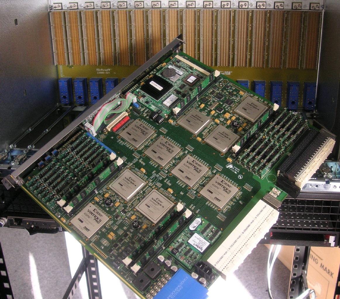
Figure 1: The CABB digital signal processing board. (Credit: Grant Hampson).
Click on image to see a larger version
The CABB DSP board is the final stage of a development process which produced the MOPS spectrometer that is now used by Mopra observers (see ATNF News 59 , June 2006). The new DSP card uses the next generation of Xilinx Field Programmable Gated Arrays (FPGAs; Virtex-4 SX55) to provide all the necessary computing power required for wide bandwidth processing.
The CABB DSP board schematic was developed using the Protel Printed Circuit Board (PCB) design package, which was also used to place all components in the layout (which doesn't sound difficult until one realises that there are 4188 components)! This design was then routed by Siart Design (India) using Cadence tools in ten weeks for a very economical price.
The Advanced Telecom Computing Architecture industry standard card cage and backplane was chosen for the project. In this system each card connects to every other card via the backplane (very good for cross correlating astronomical data). These "connections" are serial in nature and the total bandwidth available across the backplane is in excess of 6 Tbps (at 3.125 Gbps per serial data pair).
Some interesting statistics on the DSP board are: 26 layers (of which 14 are signal and 12 power/ground), dimensions 322×280 mm, track width and spacing of 0.004 inches, minimum hole size 0.012 inches, total number of nets 19217, total number of components 4188, total number of holes 22876, and total trace length 576 metres. The PCB manufacturing was handled by Entech, although it was made in Taiwan by Nan Ya PCB.
The PCBs arrived at the ATNF on 24 August 2006. It has taken one month to assemble the PCB in a piecewise fashion. The first PCB was assembled by hand, however future boards will be assembled using a recently acquired automated pick-and-place machine. A vapour-phase oven is used to reflow the FPGAs and surface mount connectors.
The CABB DSP board will also be used in the Pulsar Digital Filter Bank (PDFB) project. Firmware, including digital filter banks and correlators, has been developed for both projects, although the PDFB firmware will likely process the first pieces of astronomical data at Parkes. This will be an exciting moment for the ATNF Electronics Group!
Grant Hampson and Andrew Brown
(Grant.Hampson@csiro.au, Andrew.Brown@csiro.au)