A high-speed ADC and data transmitter board for the CABB upgrade
One of the challenges in the Compact Array Broadband Backend (CABB) upgrade project has been in developing an analogue-to-digital converter (ADC) board capable of supporting the 4,096 GigaSamples per second (GS/s) rate required for processing the 2 GHz of bandwidth demanded by the upgrade. The CABB project has aimed to use a much higher number of bits for quantising than has been traditional in the past. This is to allow for handling and potentially removing radio frequency interference in the signal processing, as well as increased sensitivity. This means that the previously developed ATNF 8 GS/s 2-bit sampler chips, as used in the Mopra Spectrometer (MOPS), cannot be used for the CABB upgrade. There are no commercially available ADC devices that meet this operation speed.
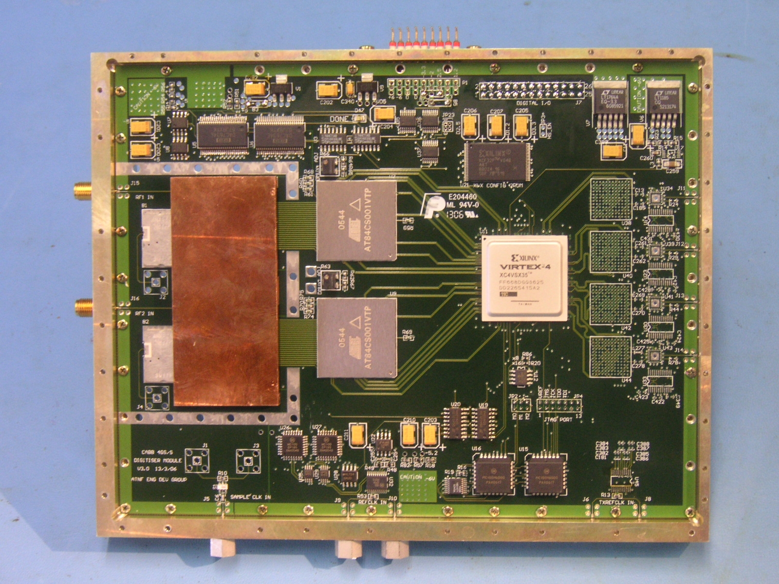
CABB ADC/data transmitter board; Photo: Paul Roberts
(click on image for larger version)
The performance achieved currently over the 2 - 4-GHz CABB intermediate frequency (IF) band at full sampling rate is a signal-to-noise ratio (SNR) of typically 38 dB (equivalent to an `effective number of bits' of ~ 6) and spurious free dynamic range (SFDR) of 39 dB. We are working on an approach to try and improve these figures further.
In addition to analog-to-digital conversion, the CABB ADC/data transmitter board also performs framing and transmission of the data. It takes the 40 Gbit/s of converted data, then frames it into 4 × 10 Gbit/s serial data streams and thence to laser driver chips for directly driving external modulated lasers. In the CABB system these are different wavelength optical data streams that are then multiplexed onto a single fibre for transport from the antennas to the control building.
The board has been designed to be as general as possible to allow it to be used in other applications apart from the CABB upgrade. It can be used as two independent 1-GHz bandwidth ADCs for instance, instead of a single 2-GHz bandwidth ADC, if required. It is being employed in this capacity in the soon to be commissioned 1-GHz pulsar digital filter bank correlator for Parkes, and for a radio transient detection experiment proposed for later this year at the Compact Array.
Paul Roberts
(Paul.Roberts@csiro.au)